Camera Selector

Vision China Shanghai 2024

Allied Vision, LMI Technologies, Chromasens, and SVS-Vistek will jointly participate in Vision China Shanghai 2024 at the TKH Vision booth. Visit us to explore the various vision solutions available from TKH Vision.


Booth number: Hall E1, 1402

8 - 10 July, Shanghai New International Expo Centre

Learn more 


Take your food sorting imaging task to the next level!

Alvium G1 cameras

DISCOVER MORE

AI-BLOX and Allied Vision

An exciting collaboration between AI-BLOX and Allied Vision. The modular edge technology platform called Blox will be integrating the new Alvium GM2 (GMSL2™ interface) cameras.

Read more

Last Time Buy for CCD cameras: August 31, 2024

Last-Time-Buy period for all Sony CCD-based sensors is ending soon. Place your order now!

Learn more!

Kudan and Allied Vision

A new exciting collaboration between Kudan and Allied Vision. The Kudan Grand SLAM software will now support the Nerian Ruby 3D depth camera and is available as part of Kudan’s Mobile Robot Development Kit for Autonomous Mobile Robots.

Learn more

High-resolution short-wave infrared cameras

Alvium SWIR cameras with Sony IMX992 and IMX993

Learn more 

Discover the Goldeye XSWIR Cameras

Goldeye XSWIR cameras with extended SWIR sensitivity up tp 2.2 µm and integrated dual-stage cooling (TEC2). 
Learn more about the award-winning Goldeye XSWIR cameras and XSWIR sensor technologies 


Find out more

Choose the right camera for your application

Go to camera selector

Take your career to the next level!

Allied Vision is looking for people like you. We are always on the lookout for ambitious professionals who share our passion for quality and innovation and who like to make our customers happy.

Find out more

Focus on what counts

We don't just develop cameras. We provide answers.

At Allied Vision, we help people achieve their goals with digital cameras for computer vision. This technology opens up a range of new possibilities for businesses throughout a broad spectrum of industries. Originally built with the needs of manufacturers in mind, our camera portfolio now extends to a wide variety of sectors including science and research, medical imaging, traffic monitoring, and sports analytics.

Given the wide variety of application challenges our customers face, we have always endeavored to offer a flexible and variable camera portfolio. This is why we design our cameras to be modular. The result is a diversity of sensors, lens mounts, filters, board-level versions, and many more options that maximize flexibility.

Discover more about Allied Vision

The image you need

Camera technology for your requirements

Our engineers design digital cameras with a large scope of resolutions, frame rates, bandwidths, interfaces, spectral sensitivities, sensor technologies, and technical platforms. We have created a modular concept to ensure that your camera adapts to requirements of your application and not the other way around.

We know how to help you find the best camera solution for your application. That includes a digital camera, but also the right lens, the right connectivity hardware and the right software interface. Our job is to reliably deliver the image you need, when you need it and how you need it.


Learn more about our pRODUCTS

From embedded to scientific

Vision solutions for your application

Do you need help

Technical information and support

Allied Vision is at your side throughout the life cycle of your image-processing project. We are here to help you integrate your camera into your system, solve software issues and ensure your system performs as it should even years after you purchased your camera.

Our specialists provide expert advice, engineering, manufacturing and support for digital cameras, their peripherals and their integration into your machine vision system.

Get an overview of helpful information and downloads!

Stay tuned!

Latest news

Defective pixels

Product News

Why buy an image sensor with pixels that need “correcting”?

Defect pixels are inherent to all CMOS and CCD sensors, due to silicon impurities and manufacturing effects. One can pay extra for fewer defects, but there is no escaping the phenomenon.

Defect pixel correction in machine vision
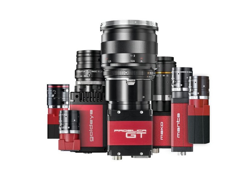
Impurities in silicon wafers and sensor production processes make it very difficult to obtain defect-free CCD or CMOS sensors. Sensor manufacturers have different grades of sensors based on the number of defective pixels. Those with few to none are classified as higher-grade and are much more expensive. Some specific applications, such as flat panel inspection, might require these higher-grade sensors. Most machine vision applications, however, do not require a “perfect” sensor and the standard grade sensors are a much more cost-effective solution.

  • Question: Hmm.  My smartphone takes great pictures, with no apparent defect pixels, and it costs less than many/most industrial machine vision cameras. Why don’t I see any defect pixels the pictures from my smartphone?
  • Answer: In fact the sensor in your smartphone has many defect pixels, but through configuration masking at build-time and algorithms in the camera’s firmware, the defects are corrected, or more properly stated, smoothed over, by “near neighbor” substitution/interpolation, to generate an image that appears defect free.
  • Question: OK, so why don’t industrial machine vision cameras sensors get the same handling as in smartphones, and spare us this whole conversation?
  • Answer: For machine vision applications, the goal is generally not to create an image that’s pleasing for a human to look at.  Rather it’s to create an image that’s interpretable by software, to take some action, e.g. “good part” vs. “bad part”, or “steer 2 degrees right”.   Depending on sensor, lens, resolution, lighting, and application, the presence of a non-continuous value amidst its neighboring pixels might be either of:

a) A defect pixel arising from the sensor, that is brighter/darker than what it should be relative to the number of photons that actually impacted that sensor position, OR

b) A genuine variance on the target surface

If it’s an instance of (b), and one is inspecting LCD TV/monitors for defects, for example, one wants to let the discontinuity pass from the camera to the software, in order to detect the candidate flaw and take appropriate action.  In the stylized illustration below, suppose the LCD was emitting nominally yellow: for the two anomalies, it would be important to know if those are from the LCD itself or from the camera sensor.   In fact one tries to design applications so that each real-world feature is “seen by” several pixels, to permit defect pixel correction, gain information, and raise efficacy, but the underlying point is hopefully clear.

So machine vision applications designers usually prefer to understand exactly what the naked sensor is generating, and to have options to engage pixel correction features under programmer control.  Perhaps an analogy back to the auto industry is appropriate: self-parking cars are now available, but as a driver I want to decide when to use that feature, whether to keep my skills sharp and park manually sometimes, or whether the situation is inappropriate to use automated-parking.  Give me options, but don’t deny me the possibility of full control if and when I want it.


Learn more
The key takeaway is that defect pixels are a fact of life, and there are effective ways to deal with them. To learn more about the technical details of pixel correction technologies and methods with Allied Vision cameras please download our application note on “Defective Pixel List Management Tool” today.

For further help on this topic, please contact us about your application goals, and we’ll be happy to recommend solutions aligned with your needs.